F21 Microprocessor Status
![]()
F21 Microprocessor Status
F21d has completed testing of the 8 bit boot instructions, 20 bit instructions, memory coprocessor, parallel port, video coprocessor, as well as power and speed tests. Analog and network coprocessors are begin tested. Results:
8 bit boot instructions: found one problem, branch on no carry always branches.
20 bit instructions: all operate as expected.
memory coprocessor: generates memory signals and has programmable timing as specified.
parallel port: operates as expected with some known shortcommings on F21d. A detailed report will be posted later.
video coprocessor: operates as planned. The current test board has DRAM memories only and is limited to generating 540x480 video at normal operating voltages. I was able to generate up to 768x482 RGB and B/W NTSC but with DRAM only the 14.3Mhz oscilator required voltage above safe voltage and required cooling of the DRAMs and would cause eventual damage to the CPU chip.
![]() The tiny GUI in the
F21 in mouse. html page and animated gif give the flavor of
this computer on a chip in a mouse. The chip emulator was upgraded
to run the Virtual Osciloscope demo ROM. Both are available for
free download at the site.
The tiny GUI in the
F21 in mouse. html page and animated gif give the flavor of
this computer on a chip in a mouse. The chip emulator was upgraded
to run the Virtual Osciloscope demo ROM. Both are available for
free download at the site.
F21 video modes tested included:
480x400
540x482
525x400
576x482
640x400
640x482 and
768x482
The current board with DRAM only limits the speed. Higher video resolutions will be tested when I put together a test board with faster memories.
Internal burst rates mips on F21d tested:
350 @ 5.0V
500 @ 5.5V
600 @ 6.0V (just currious)
700 @ 6.5V (just currious)
800 @ 7.0V (just currious)
With 7 chips (F21, 1MB UVPROM, 5x 1Mx4 DRAM) the board level power consumtion was
tested :
5ma @ 2.6V (no video)
10ma @ 3V (no video)
50ma @ 4V (no video)
100ma @ 5V (no video)
200ma @ 5V (w/ video)
300ma @ 7V (no video)
600ma @ 7V (w/ video)
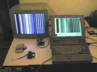
F21d displaying 768x482 on RGB monitor next to simulation on laptop.

F21d displaying 768x482 on RGB monitor captured on video camera.

Captured 768x482 RGB test pattern display
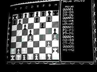
Forth chip test board running chess program
Test chess program in 320x400 b/w NTSC video.
12/28/98
F21d has passed all the initial CPU tests. It boots properly from ROM and operates as expected in DRAM. All CPU instructions appear to operate properly although F21d does not have the thermal fix that Chuck desribed in his 1998 Fireside Chat. A few critical transistors in the CPU can overheat if too many CPU instructions are loaded and executed at onpage DRAM speeds or higher because they are just a little too small. This was expected and requires some coding rules. A conservative approach to coding is to use three nops in each word to insure that the CPU has time to cool down to avoid thermal problems. Some code such as 2* 2/ can execute fully packed at 4 instructions per work, but some opcodes A A! PUSH POP will not work if packed four per memory word. These instructions may need an extra nop for each functional opcode or even only one instruction per word. With the exception of the speed restrictions imposed by having to add nops to test code the F21d CPU appears to operate well enough to permit complete testing of the coprocessors that are unique to F21.
The CPU, ROM boot, and the parallel port have been tested and work as expected. The analog I/O coprocessor, video I/O coprocessor, and serial/network coprocessor, and real time clock will be tested when I add a few more wires to the test board.
There were some unexpected delays in getting F21 back from fab and off to packaging. I plan to pick them up packaged and ready for testing later today. I plan to concentrate on lots of testing this month. I have to ship a few orders from the store and then people should realize that testing will have priority over editing web documents and replying to email or other Ultra Technology tasks.
F21d die and packaged chips are available in the store. Die will only be available until packaging. Tested chips are also listed in the store and will be shipped 12/98.
The previously published pinout was for the clcc socket with pins. This is the pinout for F21d clcc footprint.
                   Pin 1
                    |
                    v
     PA 9 8 7 6 + - 5 4 3 2 1 P0 RA RO RS
    R                                   CS
   Ni                                   P+
   No                                   P-
   PB                                    W
   Ao                                    9
   Ai                                    8
    C                                    7
    B                                    6
   A+               F21d                 5
    R               pins                 4
    G                                    3
   A-                                    2
   19                                    1
   18                                   A0
   17                                   D0
   16                                    1
   15                                    2
   14                                    3
     13 12 11 10 + + - - 9 8 7 6 + - 5 4
                 F21 Wiring Diagram
512K ROM
+      +*            BOTTOM VIEW
12    10
11    DF                   *
DE    DC      RS RA P1 P3 P5  + P7 P9 RE
DD    A7   CS RO P0 P2 P4  - P6 P8 PA So Si
A8    A6    -  +                      Ao PB
A9    A5   A9  W                      C  Ai
DB    A4   A7 A8                      +  B
-     A3   A5 A6        F21d          G  R
DA    A2   A3 A4                      13 -
RO    A1   A1 A2                      11 12
D7    A0   D0 A0                      DF 10
D6    D0   D2 D1 D4  - D6 D8  -  + DA DC DE
D5    D1      D3 D5  + D7 D9  -  + DB DD
D4    D2
D3     -
*
D0 D1 D2 D3 +  A0 A2 A4 A6 D5 D6 D7 A7  + A9 RS . wrap
 - 10 11 12 13  . A1 A3 A5  .  .  .  .  . A8 .  .
                      wrap . CS  + RS  .  .  .  .  .  .  .  .  .  .  .  .  .  -
          SIM              .  - CS CS  . WE D8 D9 DA DB DC  + DD DE DF  .  .  .

* Pin 1
10-13 are D10-D13
Connect all + and all -.  10uF between + and -
Connect labeled pins from F21:
   A0-9, D0-7, DA-12 and RO to ROM
   A0-9, D0-13, CS, RS and W to SIM
On RE, 1uF to -, 100K ohm to +

Charles Moore 8/20/98F21d was submitted to Mosis for fabrication on 8/20/98. I will post the changes to the technical specs. Most changes are timing bug fixes and power bus widening. F21d will not contain the echo timer or on chip ROM that were on F21c. They will have to be tested on a different chip. It should be back in late November for packaging. The analog I/O coprocessor will be faster and may have more resolution, it will have to be tested for accuracy and linearity. The analog I/O coprocessor now has a 2Ghz counter internally so it should be able to operate at a max of 30Msps.
I also talked to Chuck about Mosis's new .35 fab facilities. We now have the option to go to this smaller feature fab process. According to Chuck the design could use the current 2.6u tiles or rescale to 1.8u tiles. Operational voltage would be half, frequency double, amperage and power dissapation should remain the same, and temperature induced effects are expected to double. The chip would become smaller and cheaper to fabricate than in the current .8. Even in .8 we could move the pads around to reduce the chip size and fabrication cost by half.
I very much like the idea that a .35 version of F21 would have a 1 nanosecond instruction time. The memory interface coprocessor on F21 is already the bottleneck and is designed for old memories. A .35 design would really also require a new memory interface to use newer faster memories. However it will introduce so many unknowns that I am reluctant to gamble on a run. I prefer to see F21 working in .8u since that hasn't been solved yet. I think people would be very impressed by a 1 square mm 1 Ghz microprocessor with built in video card, sound card, network card, parallel port, rtc, etc, but I need a working F21 first to be taken seriously.
I have made a number of changes in the store. I invite you to stop by once in a while and look at the new products and updates etc. The latest F21 emulator is now running at a max of 3.8 F21 mips on my 120mhz pentium laptop and displaying F21 graphics programs impressively fast. I also got the first prototype the Design Your Own Processor (tm) in FPGA kit for review. I will be putting it in the store very soon.
The current plan is to submit F21d for fabrication at Mosis in August. This should bring die back for packaging in CLCC at the end of November. Recent changes in the modeling on the CAD system have given very enouraging results.
No fab run has been made on F21 since 6/97 however iTV has fabricated a number of i21 prototypes and experimented with a number of small changes to the design. The next F21 fab run has been waiting for conclusive results indictating that the final remaining bugs have been removed. iTV has been demonstrating sucessful operation of various internet appliance prototypes based on i21.
F21c was expected to be nearly perfect after a searies of nearly perfect i21 chips were produced at iTV. Unfortunately luck was not with us.
F21c exhibited several fatal design errors that prevented more than basic testing to take place. The most signifigant problem is that F21c will not write to DRAM. The chip will also not correctly execute subroutine calls and returns. Even if the boot code is written with no calls and returns it is still not possible for it to boot from ROM to DRAM because it will not write the DRAM.
Several design rule checks have been added to OKAD to catch some of the things that caused problems on F21c. Also a problem in the design of several counters in various coprocessor clocking circuits have been fixed since F21c was fabricated.
F21c prototype chips will be sold as is for experimentors who wish to attempt further testing.
Work on F21d is in progress and a prototype will be submitted to Mosis for fabrication soon. A notice will be posted on this page.
F21c failed to boot in the first tests. I didn't have enough confidence to expect it to pass a trillion instruction test, so I started with a simple 1 million instruction test program to boot and generate a video test pattern. This program failed to run and it appeared that there were problems with the subroutine calls in ROM.
Simple ROM tests are being run, and new boot code is being written and tested. It seems to be executing more ROM instructions at this time and we will try to coax it into booting into DRAM so we can test the DRAM operation of the CPU and coprocessors.
Chuck has made a simple wire wrap MISC test board that shows how little is involved in making a board by hand. F21c is being tested on a modified PCB at iTV. If F21c can be coaxed into running we will see about making a PCB for further testing.
Updated 8/25/97
F21c prototype chips came back from
Norsk Engineering Inc. 
packaged in 68 pin ceramic jlcc. 
Testing will begin today.
Updated 8/15/97
F21C prototype chips came back from MOSIS on 8/14/97. The die are now being mounted in 68 pin ceramic packages.
Updated 6/3/97
F21C prototype submission is planned for tomorrow. F21C will be the third F21 prototype design prepared by Chuck Moore and submited for fabrication by MOSIS in .8 micron CMOS. F21C will be packaged in a 68 pin plcc package similar to the production part.
F21c will offer a Real Time Clock on the chip and it will offer an echo timing circuit that will measure the time that is needed for a pulse to return from a line to an accuracy of about 100ps. (.1ns) Being able to measure a pulse reflect to a fraction of a nanosecond could be a useful feature for some specialized hardware as it could measure distance to about an inch in signals traveling at the speed of light. Perhaps people will want to experiment with lasers or radar interfaces. Chuck has suggested various uses including using it as a single bit parallel keyboard interface. If there was an inch of wire separating the keys connected parallel to ground this unit could determine which key was pressed by timing differences.
Ultra Technology Inc. will offer a development board and software for the F21C when the chips are being tested. A small quantity of prototyp chips may be available at that time testing. The yield, cost, and availability will be know after testing.
The F21c has pinout and control register changes from the F21b prototype which was packaged in a 65 pin PGA.
F21b had 3 power and 3 ground pins as did early i21 chips. F21c will have 6 power and 6 ground pins. This may be more than needed and a production part may replace some of these power and ground pins with other functions.
As with F21b F21c will not have composite video out or video input functionality. On F21b the pins were there but the circuits were not functional. On F21c there are no Vo and Vi pins. The video coprocessor on this prototype has RGB output only.
There have also been changes to the parallel port on F21c. The extra SRAM addressing lines and serial/network pins are also mapped to parallel port lines so that they can be used as parallel port i/o bits if they not being used for SRAM addressing or serial networking. It will also permit the Serial Out line to be tri-stated to support multiple network topologies.
There is also one more SRAM addressing bit A13 on P13. This allows for direct addressing of 16K words of high speed 20 bit wide SRAM to take full advantage of the 16K word sized Home Page addressing feature.
One will also notice that the die size and scale of the chip have changed. F21b had 64 pads and was twice as high as it was wide. The F21c die has 68 pads and is nearly square. F21b used .8 micron, but used larger tile sizes than F21c so the actual F21c is smaller and has more unused area on the die.
There were problems with F21a limiting execution to ROM only. F21b will execute from ROM, DRAM, and SRAM. All of the instructions worked but there were some small timing problems that require work arounds such as the addition of NOP instructions before certain instructions. There was also a problem with memory interface unit which limits which pages can be addressed from which other pages. Reliability of F21b was low, not all chips booted, reset circuit changes may coax better operation from some of the F21b prototypes. There are still some final coprocessor tests being done on F21b before the submission of F21c.
All of the CPU and memory interface bugs in F21 have been corrected in the OKAD model. There have also been various improvements to the reset and video circuits. The F21c will be prototyped in a 68-pin Ceramic LLC, similar to the production 68-pin PLCC. A second PCB will be designed to house the new F21c part.
A limited number of F21b prototype chips and F21PCBv1 are available from Ultra Technology, check for details.
F21 proved to be faster than initial expectations on instruction clock. The internal clock operates at 400 Mhz, which means instructions execute in 2.5ns plus memory load times. However the memory setup time is still 10ns which limits maximum sustained execution to around 180 MIPS.
F21c will be subitted in the summer of 96, and will return in 8 weeks. Production is still planned around year end 1996.
F21b chips were submitted to MOSIS on 12/20/95 and are expected back on 2/14/96.
F21a chips were delivered early in October by MOSIS and have been tested. Following is a list of problems found on F21a:
1. Composite video output not connected (ntsc encoder not completed)
2. T.10-T.19 shorted to data bus
3. Analog coprocessor clock permanently enabled by short
4. Parallel port short
5. Instruction sequencing problem
6. Memory timing off by 10x
Bugs 2 through 4 were shorts between circuits that were not detected by the simulator. These shorts were visible in the design to the eye when you knew what you were looking for. Scanning the design for these types of errors found only a few.
These errors were due to a problem with the way Chuck represents rectangles in his tile system. When you look at the geometric representation of the design you can see that the poly regions expand to fill in the areas between tiles so that poly makes nice filled in areas. But at other times poly is the line of conduction so if two different poly lines are on adjacent tiles they are shorted. If they are in different circuits they should should not look like that and the simulator does not catch it. Searching the chip visually in the simulator for this problem was quite interesting.
As for each of these problems:
1. Composite video output not connected, and the composit (ntsc) encoder not completed at this time.
Chuck never finished the ntsc encoder because he was in the process of redesigning it. He didn't like the quadrature composite video encoder because it introduced too much noise in higher harmonics. This resulted in some colors that are hard to use for anything in MuP21. But Chuck has been trying some different things on other chips and just has not put a composite video encoder into F21 yet. The RGB and composite outputs run at the same time anyway. It is a specialized D/A with RGB outputs and some form of encoded composite version of the RGBi signal on the yet to be completed on F21 composite video output line.
2. T.10-T.19 shorted to data bus
The problem was found by Chuck and identified as a design problem about the time the F21 was submitted to MOSIS. I could have canceled the fab run since it had only started, but we knew that the 10 top bits on the data bus were permanently shorted to the T register. This limited my expectations to testing the thing in 8 bit instruction mode if it was going to work that well.
3. Analog coprocessor clock permanently enabled by short
I didn't see this one, but Chuck said that the short in the circuit from the analog coprocessor count down clock was permanently enabled on the bus. After 300ms of operation the analog coprocessor would start reading and writing on the data bus and no more access for the CPU would occur. The address and data bus would just show this steady pattern. All testing had to be done with short programs that executed while the cpu had control and the results examined post mortim on a logic analyzer.
4. Parallel port short
One more short not apparent from testing in the OKAD simulator. These were simply human errors in the design layout. The port had been tested in the simulator but did not work properly.
5. Instruction sequencing problem
Chuck reported that you could not get a memory access instruction after a jump instruction due to an internal ALU/CPU/Memory interface internal sequencing problem in the design.
6. Memory timing off by 10x
Chuck tried a whole new way of timing the memory interface. He make it programmable and it worked, but he was off on one estimate and it charged up this timer about 10x slow. These curves get pretty flat pretty fast and he hit it too low. The cad system uses an innovative approach of simulating the analog operation of the entire chip. Chuck has changed from voltage simulation to current integration simulation in the latest OKAD. This allows more accurate simulation of slowly changing analog processes in the OKAD simulator. I expect F21b should be closer to the corrent timing mark.
In addition to these known problems there were also some future "tweaks" that were planned for the second prototype but were not done on F21b because they involve results from more detailed testing of I/O coprocessors than was possible with the first prototype. I would like to be able to run the serial network as fast as the design will support and this will require tweaking because Chuck has not done these high speed serial signals yet.
A third prototype will be done. If production is done by MOSIS the price will be higher, but if it moves offshore then another prototype will be done.
![]()