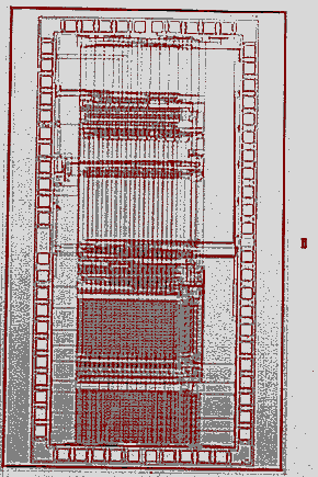
F21 is being fabricated .8 micron CMOS technology using the HP process at Mosis. F21 is being prototyped in a 68 pin ceramic package similar to the 68 pin PLCC that will be used for production. Click here to see the F21 current F21 status, or click here to see the current F21b prototype Printed Circuit Board.
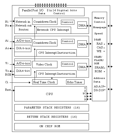
The F21b microprocessor contains a It will access to 3 memory spaces, one megaword of 20 bit wide DRAM, 8K words of 20 bit wide fast SRAM, and one megabyte of 8 bit wide PROM, SRAM, FRAM, or PCMCIA CARD memory for booting. It will interface directly to 5 1Mx4 or 265Kx4 DRAMS and/or 3 8Kx8 high speed SRAM. A system can be built with only 5 or 7 chips. Memory timing for the three memory spaces are: 150ns or 250ns for 8 bit SRAM, 40ns onpage and 140ns offpage 20 bit DRAM, and 12ns or 25ns for 20 bit fast SRAM. All memory timings are adjustable within a 40% speedup range. The chip also provides a 8 bit wide parallel I/O port decoded and latched on chip.
The memory interface processor provides memory access to all processors giving lowest priority to the CPU. The I/O coprocessors can be turned on or off by the CPU, and can run continuously executing their own instructions, or can interrupt the CPU to process their data buffers or instructions.