PCB F21V1.PCB for F21b
![]()
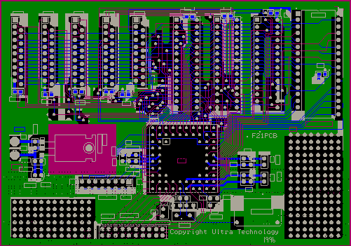
PCB F21V1.PCB for F21b
The first F21 PCB was returned from Acculay and is being populated for testing. The design is 3x5in 4 layer PCB with 1 F21b, 3 8Kx8 SRAM, 5 1Mx4 DRAM ZIP, 1 128kx8 ROM, clock, power regulator, and prototyping area. It is designed to provide a simple and stable test platform for the F21b prototype chips. The PCB schematic, library components, details, and production results will be made available at this web site.
The initial layout was done by:
Edward Matejowsky.
http://www.ozemail.com/au/~eddiema/index.html
Review and additional help from Dr. C. H. Ting and Chuck Moore.
![]()
 F21V1.PCB 3/4/96